VSP-P1 NanoPrinter
VSP-P1 Nano Printer
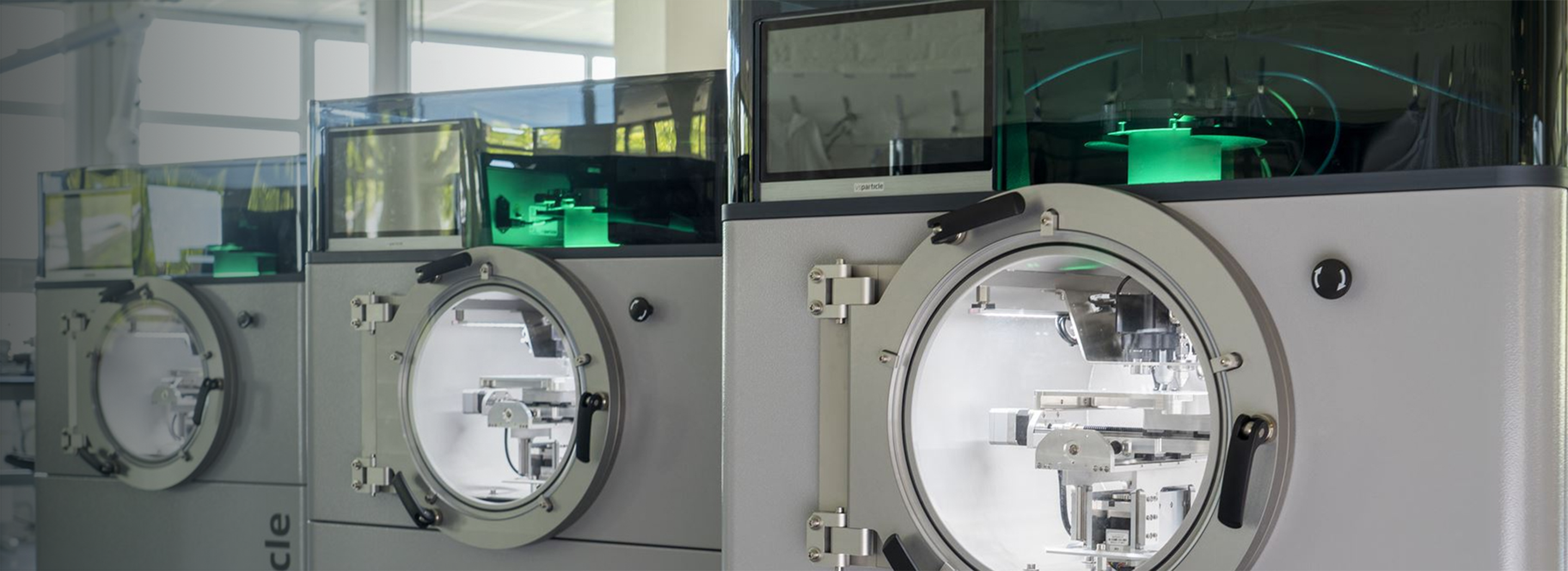
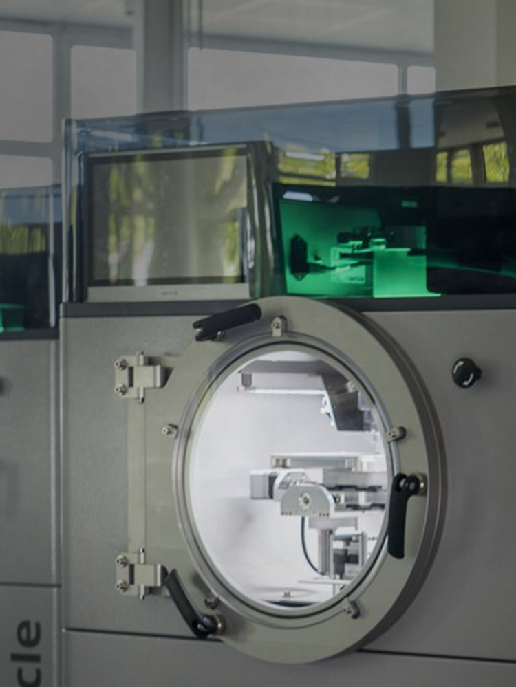
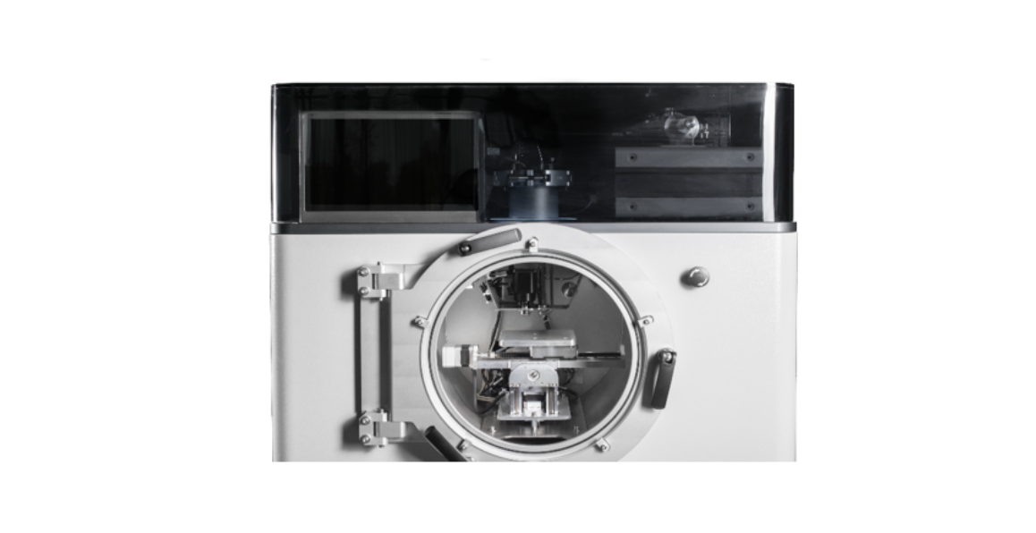
The VSP-P1 NanoPrinter enables you to locally print inorganic nanostructured materials with unique properties.
  • VSP-P1 NanoPriNter
  • Product Display
  • Product Function
  • Product Function
  • Customer Testimonials
  • Download Center
VSP-P1 NanoPrinter
VSP-P1 NanoPriNter
Product
Overview

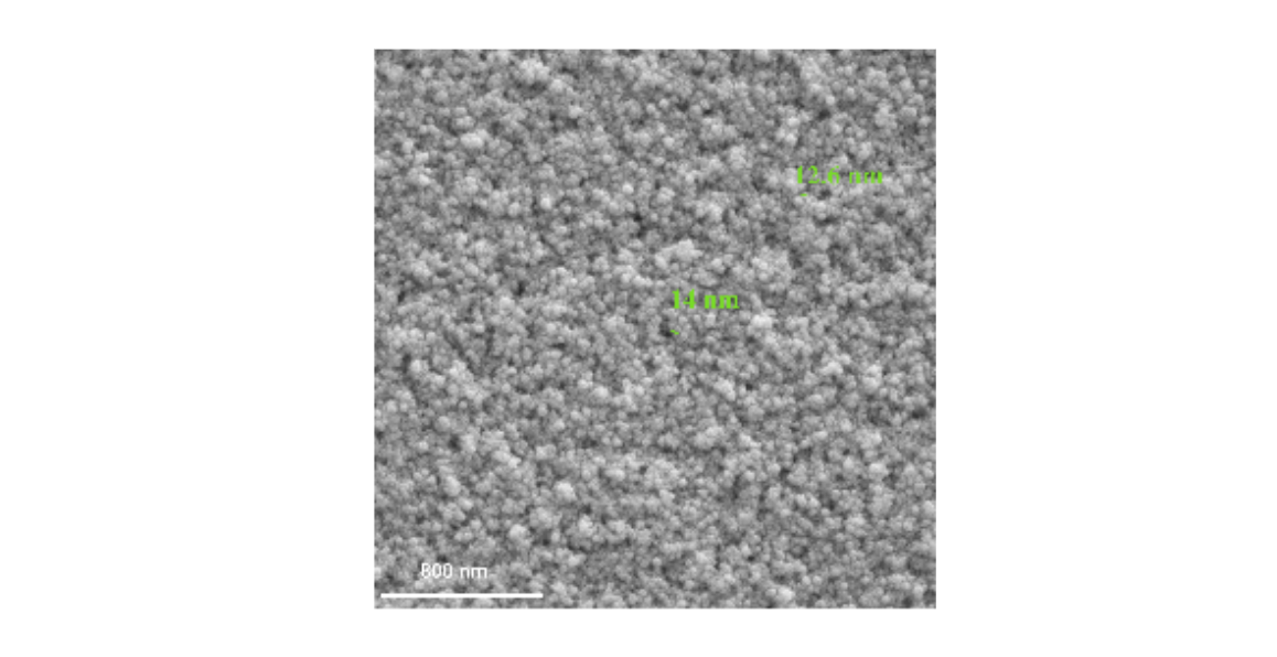
Easily and controllably print nanostructured layers, the VSP-P1 NanoPrinter is the ultimate prototyping and R&D platform for materials development and small-scale production testing. Based on stamping deposition of spark ablative materials, the system employs additive manufacturing to simplify the production of nanoporous films and layers with high surface-to-volume ratios.

Basic
Parameters
Print dimensional accuracy
10 μm
Print lineweight dimensions
100 μm -1 cm
Coating structure
Nano porous structure
Coating thickness
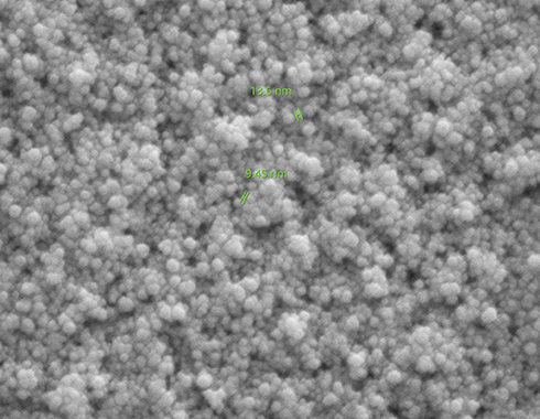
Sparse clusters (100 nm )- a few microns
Maximum print area
15 x 15 cm
Abutment dimensions
Max. 20 x 20 cm
Target
Suitable for any conductive or partial semiconductor material
Carrier gas
ArorN2 (recommended purity 99.999%), which binds to trace amounts of reactive gases such as 02 or H2
Operating conditions
Room temperature or low vacuum
Initial nanoparticle size
1-20 nm
Nanoparticle yield
0.01- 20 mg/h
Product Display
  • Modular combination 01

    1-2 sets of VSP-G1 nanoparticle generator can be built-in as a material source;

    It can be used with VSP-S1 particle size screening deposition module for printing fixed particle size.

  • True dry aerosol deposition 02

    The particles are produced entirely from VSP-G1 without any ink components added;

    The particles are produced by physical methods and do not contain any chemical additives.

  • Ultrafine nanoparticle print deposition 03

    Rapid deposition of alloys or mixtures of heterogeneous nanoparticles;

    Aerosol typical particles have an initial particle size < 20 nm

Modular combination

1-2 sets of VSP-G1 nanoparticle generator can be built-in as a material source;

It can be used with VSP-S1 particle size screening deposition module for printing fixed particle size.

  • Modular combination
  • Dry aerosol deposition
  • Ultrafine nanoparticle print deposition
True dry aerosol deposition

The particles are produced entirely from VSP-G1 without any ink components added;

The particles are produced by physical methods and do not contain any chemical additives.

  • Modular combination
  • Dry aerosol deposition
  • Ultrafine nanoparticle print deposition
Ultrafine nanoparticle print deposition

Rapid deposition of alloys or mixtures of heterogeneous nanoparticles;

Aerosol typical particles have an initial particle size < 20 nm

  • Modular combination
  • Dry aerosol deposition
  • Ultrafine nanoparticle print deposition
Product Function
Product Function
  • 01 Control nanodeposited layer thickness
  • 02 Patterned printing
  • 03 Nano porous coating deposition

The parameters that affect the layer thickness are:


• The distance from the nozzle to the substrate         • Ablation power         • Printing speed


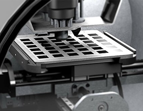
After the nanoparticles are generated by VSP-G1 spark ablation, the aerosol stream generated using coarse vacuum acceleration passes through the nozzle. Therefore, the driving force of impact printing onto the substrate is the pressure gradient between the VSP-G1 system and the deposition chamber.With XYZ stage control, microscope camera modules, and an intuitive user interface, specific patterns can be printed. You can run a script through the user interface to determine the desired print mode. Series production with different or modified scripts, complex patterns and multiple samples.


Unlike traditional thin film deposition technology, VSP-P1's aerosol direct writing technology can deposit nano-coatings in selected areas and use fine nozzle movement to achieve thickness control, which is well suited for non-semiconductor nanofilm applications.


Application Instance
Product Function
01 Development of highly efficient catalyst coating films

PEM 水电解是最近引起广泛关注的应用之一。然而,其市场应用受到阻碍,因为 PEM 电解槽依赖于使用稀有且昂贵的贵金属催化剂,例如铱。作为应对这一挑战的解决方案,使用 VSPARTICLE 的技术开发铱催化剂涂层膜。结果证明,与市售标准样品相比,气溶胶打印方法所需的催化剂负载量更少,降低了五倍,Ir 特定的功率密度降低了一个数量级并且耐久性良好。

• 出色的性能,催化剂负载量减少了一个数量级

• 单步无墨涂布工艺

• 卓越的耐用性和使用寿命性能

02 Rapid electrocatalyst (model) screening

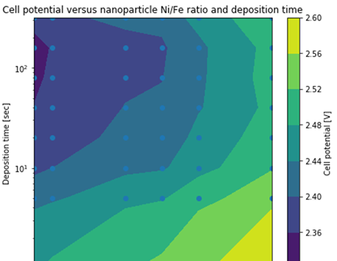
使用连接到 VSP-P1 NanoPrinter 的两个 VSP-G1 纳米粒子发生器,可以进一步加快筛选多元素电催化剂的能力。为了说明这种设置的可能性,VSPARTICLE 与 Avantium 合作,筛选了 64 种不同的OER 用Ni-Fe 电催化剂。VSPARTICLE 的技术使研究人员能够筛选 64 种不同电催化剂组合物的性能,显着加快新型电催化剂的开发。

03 Gas sensor research

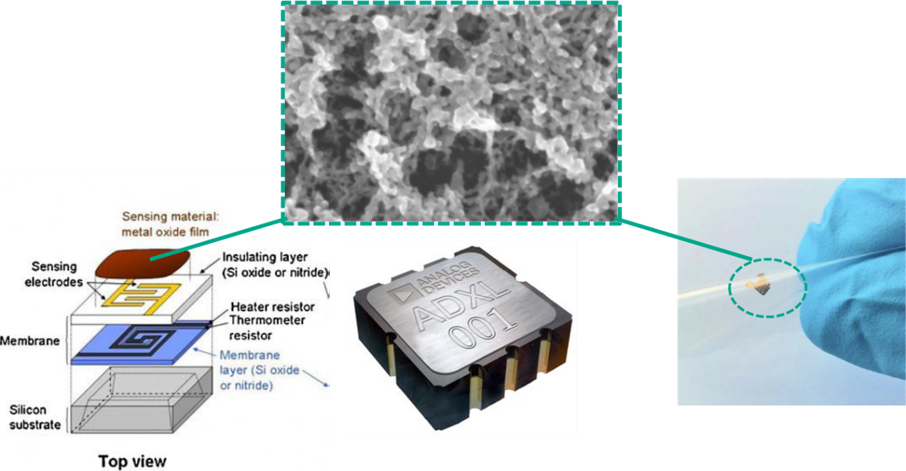
通过为 VSP-G1 纳米粒子发生器配备我们最先进的 VSP-P1 纳米印刷沉积系统,可以快速生产各种基于 SMO 的传感器。这种配置使研究人员能够轻松沉积不同的金属氧化物,并制备具有不同初级粒径和层厚的 SMO 传感器。通过使用带有合金电极和/或多个 VSP-G1 纳米粒子发生器的 VSP-P1 NanoPrinter,还可以轻松制备混合和/或掺杂的金属氧化物,并能够调整初级粒径和元素组成

04 Surface enhanced Raman scattering

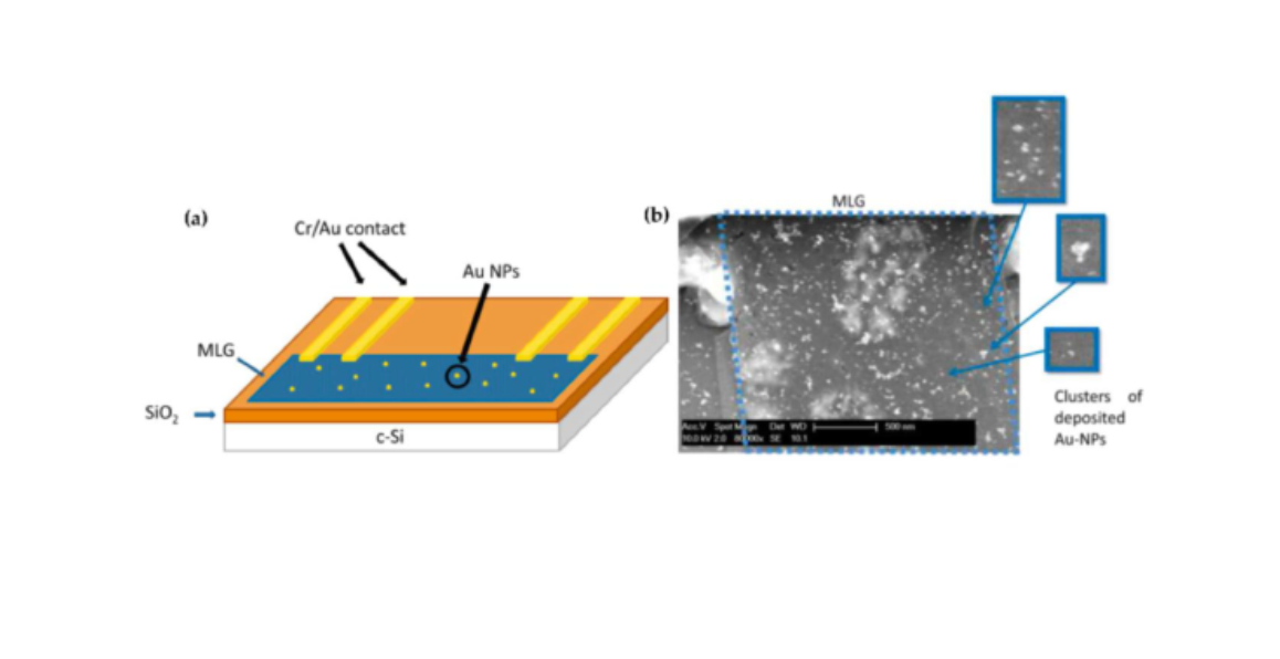
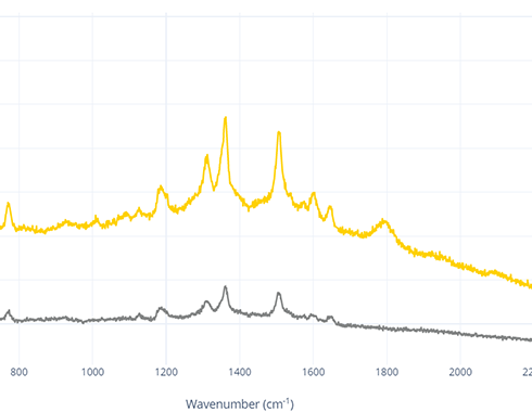
表面增强拉曼散射( SERS ) 是一种表面敏感技术,可通过吸附在粗糙金属表面上的分子或纳米结构(如等离子体磁性二氧化硅纳米管)增强拉曼散射。利用VSP-P1在石英玻璃基底表面沉积Au-Ag图案,实现最为简便的拉曼增强效果。

Testimonials
Customer Testimonials
  • “With the use of the VSP-P1 NanoPrinter I have been able to implement all my ideas when it comes to decorating biosensors with nanoparticles. I really like that I can choose between a lot of different parameters and get exactly the size and quantity of nanoparticles that I desire but also combine different materials.”

    Merlin Palmar Master's in biomedical engineering at Delft University of Technology, Bioelectronics department
  • “The versatility and material flexibility of the nanomaterials printer allows us to print a wide range of nanomaterials on finished microelectronics devices. We are now able to decorate gas sensors and deposit on thin membranes and other fragile substrates without putting too much effort in finding a good recipe. Because it’s so simple to test something new, we can think of new experiments often and perform them the next day!”

    PhD Candidate Joost van Ginkel Department of Microelectronics TUDelft
Download Center
Download Center

If you want to know more product information, please fill in the following information to download the product manual.

  • *
  • *
  • *
  • *
Reserved information
预留信息

如果您想要了解更多产品信息,请填写以下信息下载产品手册, 我们收到您的信息后将第一时间回复您。

  • *
  • *
  • *
  • *