Conventional transmission electron microscopes (TEM) primarily act as an imaging tool to characterize structures of materials.
In the last few years, state-of-the-art TEMs have enabled atomic resolution imaging and analysis, which has been achieved through the use of image or probe aberration-corrected TEMs. The performance of these TEMs as an imaging tool has proven to be extremely valuable in identifying various material structures.
However, these conventional TEMs are still unable to support the whole research process. The reason is that conventional TEM is unable to replicate real-world environmental conditions (heating, gas, liquid, etc.) as the sample is always introduced into a high vacuum, static environment. This fundamentally limits the value and obtainable benefits of a TEM.
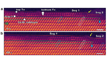
Observing processes ‘on-site’ as they are occurring and under changing external stimuli is the ultimate goal of in-situ, time-resolved techniques.
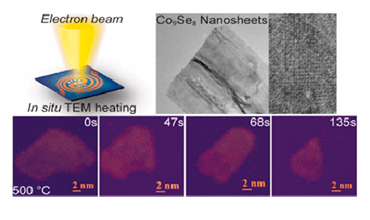
DENSsolutions utilizes MEMS devices, the core of our systems, to control the sample’s environmental surroundings and replicate real-life application conditions inside your TEM (see image above). The introduction of in-situ capabilities into a TEM, transforms the system from a static imaging tool into a multi-functional laboratory.
With DENSsolutions in-situ microscopy solutions, researchers are now able to characterize structures, measure properties, evaluate performance and optimize processes & synthesis.
If you want to know more about the product information, book a sample or consult the after-sales service, you are welcome to call our hotline 400 857 8882 or leave us a message online, we receive your message will be the first time to reply to you.